

Supporting Power Semiconductors
and Advanced Packaging Processes
Higher Reliability,
Greater Productivity
Enabled by Non-Contact Metrology
High-Throughput, High-Precision Measurement
3D Measurement of Ultra-Fine Features
(L/S = 2/2 μm)
(L/S = 2/2 μm)
Automation and Efficiency Through Integration with Handling Systems
Easy-to-Use
IR Transmission Inspection
IR Transmission Inspection
Mitutoyo Solutions
for the Semiconductor Industry
for the Semiconductor Industry
Solutions for
Advanced Semiconductor Packaging
Advanced semiconductor packaging plays a critical role in the evolution of AI and high-performance devices.
To enable high-speed signal transmission and reduce power consumption, multiple chips are integrated into 2.xD and 3D architectures using interposers. At the same time, feature sizes continue to shrink and designs become more complex.
As device complexity increases, manufacturing is shifting from wafer based processes to panel based processes to improve efficiency and scalability, accelerating R&D and innovation.
As equipment scales to support these panel based processes, measurement systems must deliver both high throughput and highly accurate positioning.
With extensive experience in semiconductor packaging metrology, Mitutoyo helps improve quality and reliability through advanced measurement technologies.
To enable high-speed signal transmission and reduce power consumption, multiple chips are integrated into 2.xD and 3D architectures using interposers. At the same time, feature sizes continue to shrink and designs become more complex.
As device complexity increases, manufacturing is shifting from wafer based processes to panel based processes to improve efficiency and scalability, accelerating R&D and innovation.
As equipment scales to support these panel based processes, measurement systems must deliver both high throughput and highly accurate positioning.
With extensive experience in semiconductor packaging metrology, Mitutoyo helps improve quality and reliability through advanced measurement technologies.
Facing These Challenges?
Challenge 1
Limitations of Optical Microscopy for Fine Features
As interposer wiring becomes finer and aspect ratios increase, conventional optical microscopy alone is no longer sufficient for accurate evaluation. There is also a need to measure large panels up to 500 mm in size.
Challenge 2
Need for Non-Destructive Internal Inspection During Production
X-ray CT inspection requires time consuming pre-processing, while SAT inspection requires immersion in water. Both methods make it difficult to integrate inspection into in-line processes.
Challenge 3
Need for Accurate Measurement of Design Compliance
While visual inspection systems are used for external checks, accurately measuring size and positional accuracy remains a challenge. Conventional measurement systems are often too slow.
Solve These Challenges
with Mitutoyo Solutions
Solution01
High-Precision 3D Measurement of Ultra-Fine Features
(L/S = 2/2 μm)
(L/S = 2/2 μm)
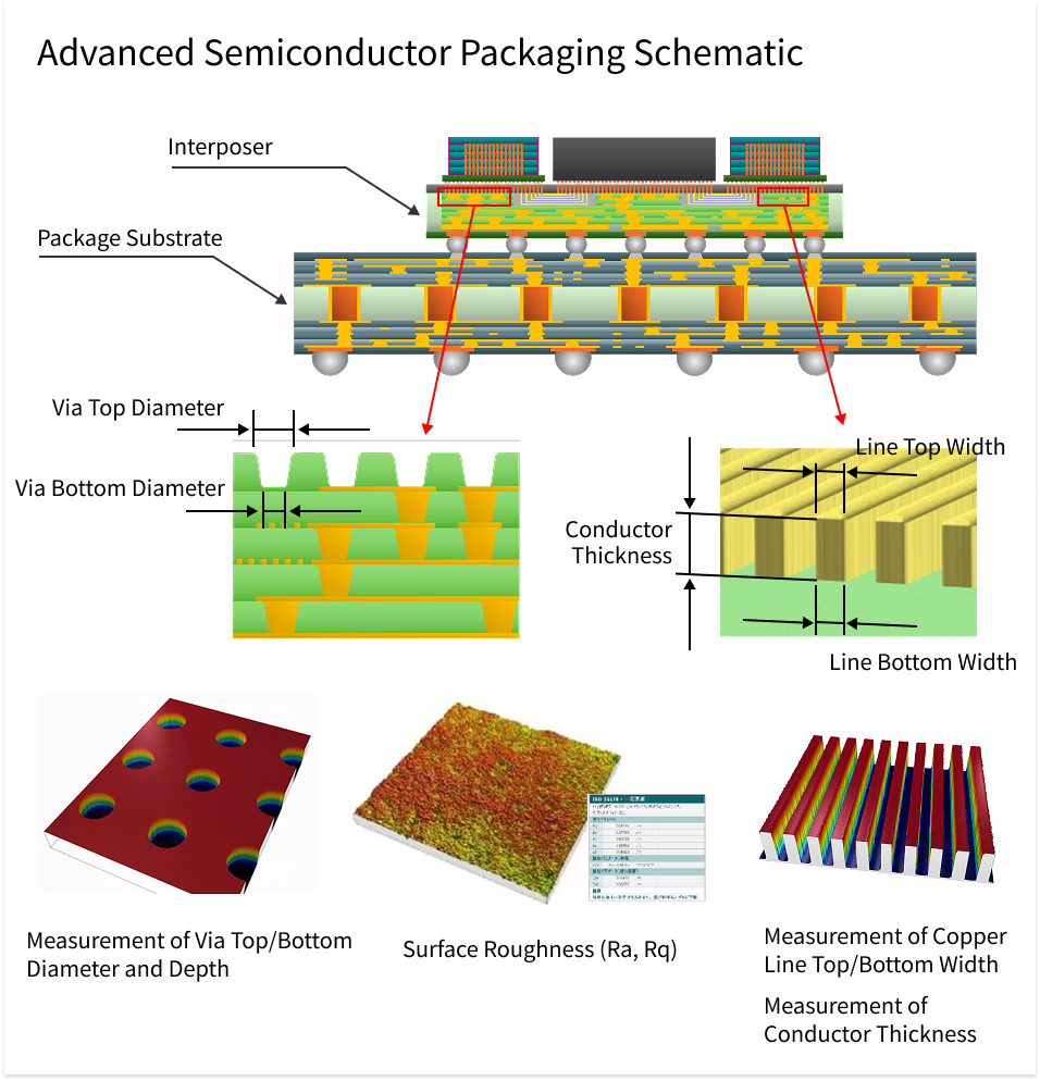
Supports high precision 3D measurement of high-aspect-ratio line and space patterns (L/S = 2/2 μm), small diameter vias, and micro bumps.
Also measures surface characteristics and roughness of encapsulation and interlayer materials across a wide range, helping improve quality control throughout the manufacturing process.
Also measures surface characteristics and roughness of encapsulation and interlayer materials across a wide range, helping improve quality control throughout the manufacturing process.
Solution02
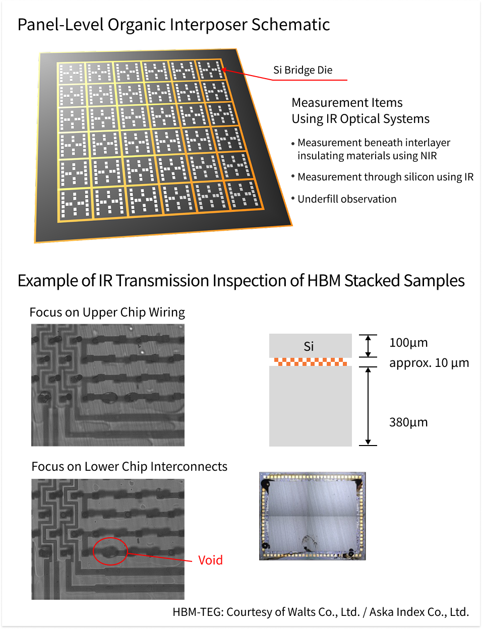
Easy-to-Use IR Transmission Inspection
Evaluating undefill under silicon using special optics to view through interlayer insulating materials.
Embedded interposers and component integrated substrates can be measured nondestructively, eliminating the need for time consuming pre-processing required by X-ray CT or SAT. This enables in process quality control.
Embedded interposers and component integrated substrates can be measured nondestructively, eliminating the need for time consuming pre-processing required by X-ray CT or SAT. This enables in process quality control.
Solution03
Redefining Measurement with High Throughput,
Ultra-High Precision Technology
Ultra-High Precision Technology
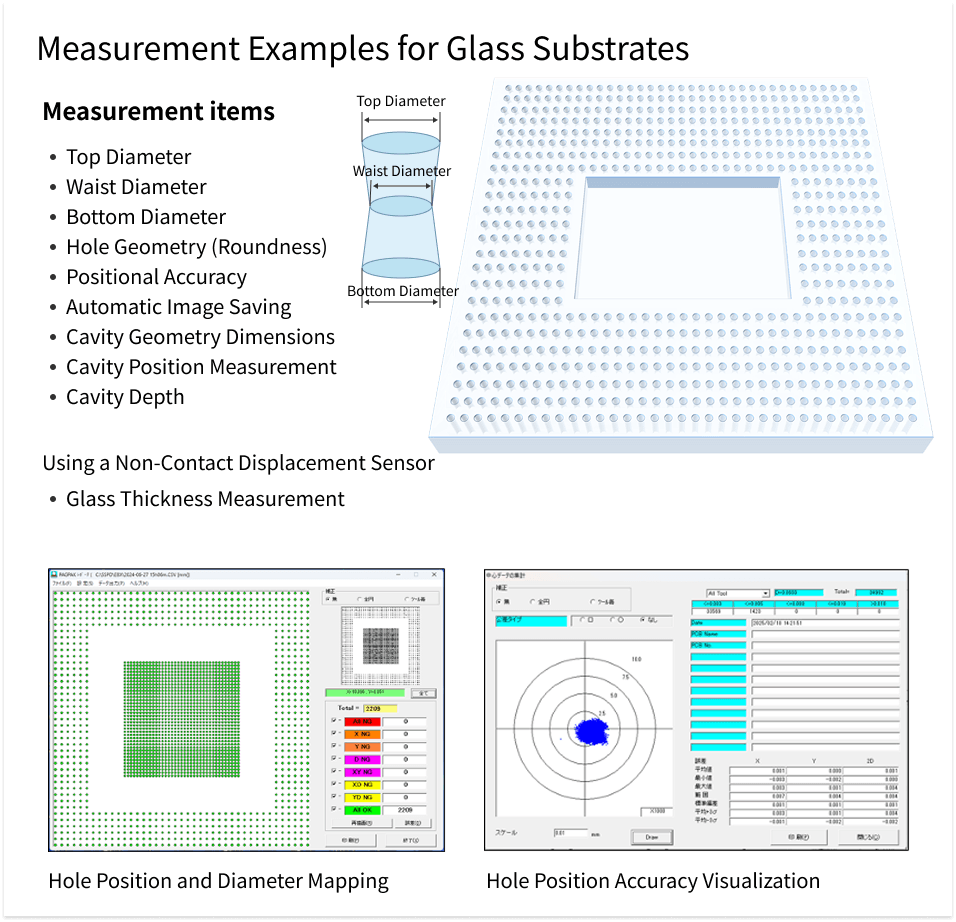
High-throughput measurement expands the capabilities of conventional systems, supporting a wide range of applications including vias in glass substrates, Cu posts, micro bumps, and positional accuracy of mounted components.
It also verifies compliance with design rules and provides absolute dimensional measurement traceable to national standards, helping improve yield and reliability.
It also verifies compliance with design rules and provides absolute dimensional measurement traceable to national standards, helping improve yield and reliability.
Key Benefits
- 1Automated Measurement of Previously Difficult-to-Measure Ultra-Fine Features in Panel-Level Interposers
- 2In-Process IR Inspection Without Product Damage
- 3 High Precision, High Throughput Measurement to Improve Advanced Packaging Quality
Solutions for
Power Semiconductors
Power semiconductors play a critical role in advancing a decarbonized society, driven by trends such as vehicle electrification and the expansion of green energy.
As devices become smaller and more efficient while supporting higher power capacity and voltage, new materials such as SiC and GaN are increasingly being adopted.
In this evolving landscape, Mitutoyo’s QV Pro, equipped with the Stream Function and Tracking Auto Focus (TAF), enables high throughput, high precision measurement of the position and tilt of tens of thousands of dies on a substrate.
This helps improve product performance and reliability.
As devices become smaller and more efficient while supporting higher power capacity and voltage, new materials such as SiC and GaN are increasingly being adopted.
In this evolving landscape, Mitutoyo’s QV Pro, equipped with the Stream Function and Tracking Auto Focus (TAF), enables high throughput, high precision measurement of the position and tilt of tens of thousands of dies on a substrate.
This helps improve product performance and reliability.
Facing These Challenges?
Challenge 1
Time-Consuming Measurement of Die Position and Tilt
Accurate measurement of die position and tilt across all dies is required, but conventional systems take too much time, increasing lead time, while optical inspection systems lack sufficient accuracy.
Challenge 2
Pin Misalignment Caused by Substrate and Lead Frame Warpage
Warpage of substrates and lead frames can cause pin misalignment, leading to frequent line stoppages and reduced productivity.
Challenge 3
Low Efficiency in Manual Workpiece Handling
Manual loading and unloading of workpieces result in long downtime, limiting productivity and preventing unattended operation.
Solve These Challenges
with Mitutoyo Solutions
Solution01
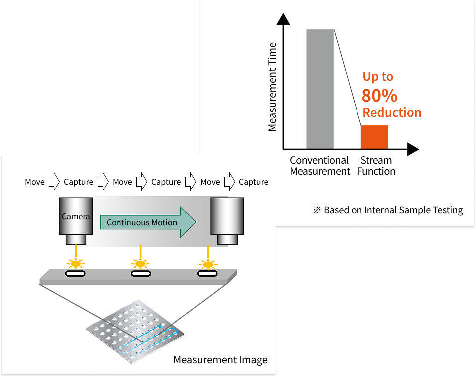
QV Pro’s Stream Function Reduces Takt Time
for Full-Die Position Measurement by Up to 80%
for Full-Die Position Measurement by Up to 80%
The QV Pro series features strobe illumination as standard across all models.
By synchronizing stage movement with strobe illumination, the Stream Function enables continuous measurement without stopping the system.
This significantly reduces the lead time required to acquire position data for all dies.
By synchronizing stage movement with strobe illumination, the Stream Function enables continuous measurement without stopping the system.
This significantly reduces the lead time required to acquire position data for all dies.
Solution02
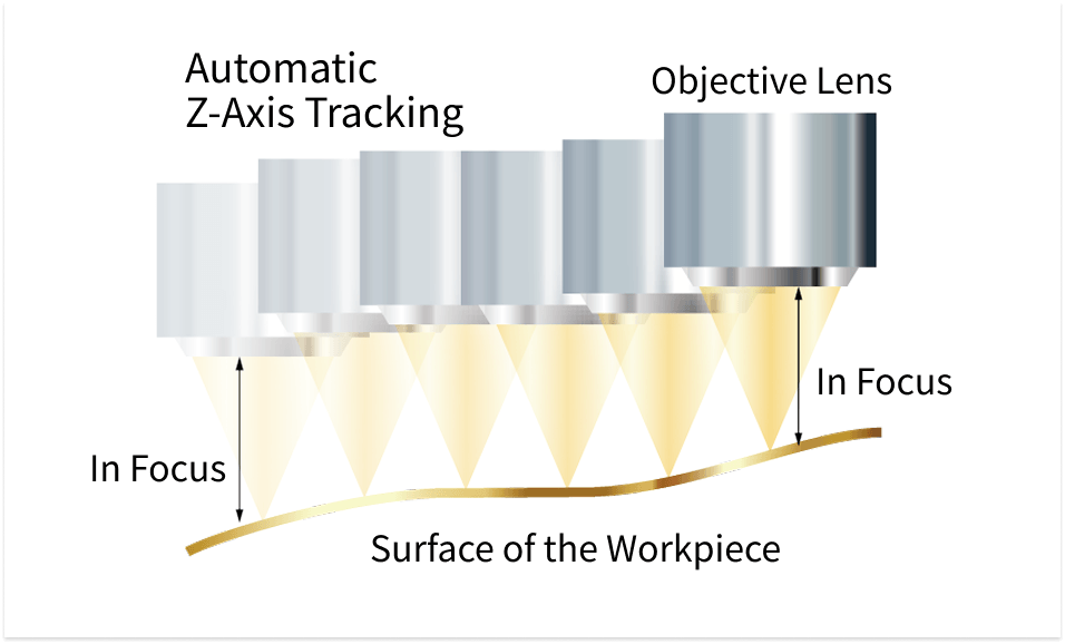
QV Pro’s Tracking Auto Focus (TAF) Instantly Adjusts to Maintain Focus Regardless of Warpage or Tilt
The laser based Tracking Auto Focus (TAF) function enables real time tracking of surface variations in the workpiece.
It instantly adjusts focus to compensate for substrate warpage and die tilt, reducing line stoppages caused by focus misalignment.
It instantly adjusts focus to compensate for substrate warpage and die tilt, reducing line stoppages caused by focus misalignment.
Solution03
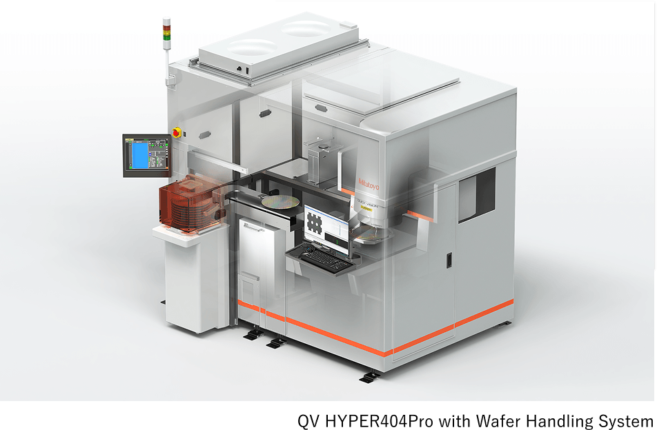
Boost Measurement Productivity with QV Series and Automated Handling Systems
Mitutoyo offers automated sample handling systems using magazines and FOUPs.
Automation of workpiece transfer improves productivity while reducing contamination risks to samples.
Automation of workpiece transfer improves productivity while reducing contamination risks to samples.
Key Benefits
- 1Non-Stop Measurement with Stream Function Enables High Throughput
- 2TAF Enables Real-Time Surface Tracking Despite Warpage and Tilt
- 3Integration with Automated Handling Systems Improves Measurement Productivity
Solutions for
Build-up Substrates
As semiconductor performance continues to improve, chiplet architectures and advanced packaging technologies are gaining increasing attention.
Mitutoyo’s QV-WLI utilizes white light interferometry to enable high precision measurement of ultra fine features such as vias, fine lines, and surface roughness in packaging processes.
This helps improve product quality and reliability.
Mitutoyo’s QV-WLI utilizes white light interferometry to enable high precision measurement of ultra fine features such as vias, fine lines, and surface roughness in packaging processes.
This helps improve product quality and reliability.
Facing These Challenges?
Challenge 1
In-Process Measurement of Laser Micro-Via Diameter and Depth
Accurate measurement of bottom diameter and internal conditions of micro vias is required to support process control.
Challenge 2
In-Process Control of Line Width and Conductor Thickness
Line width and spacing are currently measured using SEM, but a simpler in process measurement method is needed.
Challenge 3
Low Efficiency in Manual Workpiece Handling
Manual loading and unloading of workpieces cause long downtime, limiting productivity and preventing unattended operation.
Solve These Challenges
with Mitutoyo Solutions
Solution01
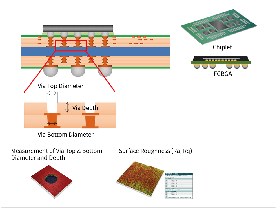
Enable In-Process Control of Small-Diameter
Via Diameter and Depth (Ø20 μm)
Via Diameter and Depth (Ø20 μm)
Enables measurement of via diameter and depth in laser-drilled vias used for vertical interconnections in package substrates.
Small-diameter vias (Ø20 μm) can also be measured, enabling features previously inspected using SEM to be measured directly within the manufacturing process.
Small-diameter vias (Ø20 μm) can also be measured, enabling features previously inspected using SEM to be measured directly within the manufacturing process.
Solution02
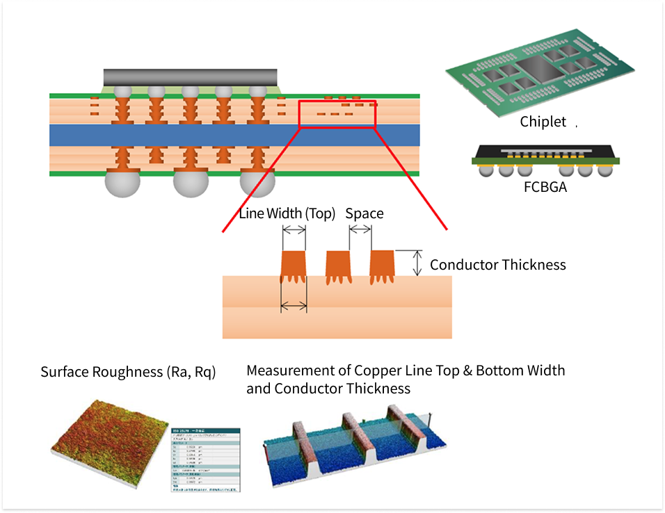
In-Process Control of Line Width, Spacing,
Conductor Thickness, and Surface Roughness
Conductor Thickness, and Surface Roughness
QV-WLI uses white light interferometry to measure line width, spacing, and conductor thickness formed through SAP processes (semi-additive processes), such as resist patterning and plating.
Solution03
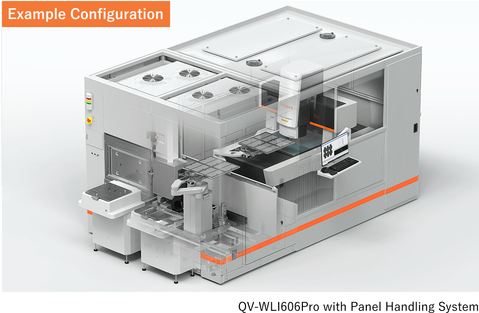
Boost Measurement Productivity with QV Series and Automated Handling Systems
Mitutoyo offers automated sample handling systems using magazines and FOUPs.
Automation of workpiece transfer improves productivity while reducing contamination risks.
Automation of workpiece transfer improves productivity while reducing contamination risks.
Key Benefits
- 1Non-Stop Measurement with the Stream Function Enables High Throughput
- 2TAF Enables Real-Time Surface Tracking Despite Warpage and Tilt
- 3Integration with Automated Handling Systems Improves Productivity